128KB in a 64KB Bag
There are four (accessible) ROM sockets on the TEMPEST GRiDCase, all 28 pin DIL and with very little clearance up top for the bunch.[1] If you've got some EPROMs and a programmer, ROMBUILD.EXE, and MS-DOS' system files, then you're well on your way to booting from ROM rather than floppy.
Three files are required to boot MS-DOS 3.2: IO.SYS, MSDOS.SYS, and COMMAND.COM. Collectively, those three files are 68kb. Unfortunately, the largest capacity 28 pin EPROM[2], the 27512, is 64kb, ergo booting from ROM would require two EPROMs and two of the four available ROM sockets. One could, and should fill the remaining space on that second EPROM with needed programs, (FORMAT.EXE,MODE.EXE, etc.). But, given such a low memory limit, it becomes difficult to determine which programs should be considered indispensable, and therefore burned to ROM, and which should be relegated to life on a floppy.
Larger capacity ROMs were created, in a 28 pin package, but these were masked ROMs and purchasing a run of them must have been, (this might be obvious to anyone with a background in electronics manufacturing), very expensive; I've seen GRiD-branded ROMs, add-ons which I assume were not inexpensive, but with label stickers affixed that failed to obscure the EPROM's make/model.[3]

The 27512 is a 512-Kilobit (64K x 8-bit) EPROM. (512 * 1024) / 8 = 65,536, which means there are 65,536 available locations in which to store a byte. Or rather, for each of the 65,536 address inputs applied, the 27512 returns eight output bits[4]. In order that those eight bits be read out onto the eight data lines, the ROM must possess enough pins, A0...A15, to handle the 16-bit input address, (216 = 65,536). The address is arranged so that A15 is the MSB and A0 is the LSB.[5]
As 00000000000000002 = 000016 and 11111111111111112 = FFFF16, the resulting address range can be written as 0x0000, 0xFFFF.
If that memory capacity were to double, as would be the case if using an HN62321, a 1M (128K x 8-bit) Mask ROM, in place of the 27512, then not only would the number of storage locations increase by a factor of two, (1024 * 1024) / 8 = 131,072[6], but also the range of addresses needed, 0x00000, 0x1FFFF. Consequently, a 17-bit input address, (217 = 131,072), and an additional address line, A16, would be required.

Compared side by side, one can see that the only meaningful difference between the pinout of the 27512 and the HN62321 is pin 22.[7]
The "output enable" function of the 27512's O̅E̅/VPP pin, as the name might suggest, enables output on the data lines when switched logic low. When switched logic high, it disables output; those pins become input lines for programming the device.
The HN62321, for obvious reasons, does not need a pin with which to switch its data lines between input/output and instead uses pin 22 for the additional address line, A16.

The 27C010 is, like the masked ROM, 1M (128K x 8-bit) , but in a 32 pin DIP package. It is pin compatible with the 27512 and therefore, one pin off from the HN62321.
(128kb EPROMs exist which are pin compatible with 1M Mask ROMs (28pin type), such as the HN27C301, and if used would mean that a very simple adapter could be fashioned from a couple of IC sockets).
Between the 27C010 and HN62321, the only pins in direct conflict are 24 and 22. As an adapter, in this case, would only ever be used to read the EPROM, it can be assumed that O̅E̅ should always be active, and with a jumper, brought to VSS. The 27C010's pin 2, A16 would then be wired to pin 22 on the ROM socket.
This leaves VPP, VCC, and P̅G̅M̅ on the 27c010, pins 1, 32, and 31, respectively.
According to the 27C010's datasheet, when reading the EPROM, VCC = VPP = 5.25 V. Additionally, P̅G̅M̅, used to enable input during programming, should also be driven high, which is fortunate as its pin, 31, lives next to VCC.

The 27C010's pin 30, NC, can be handled in different ways. For prototyping an adapter or perhaps as a quick fix in a system that just needs a ROM replaced, pin 30 could be left alone, i.e., bent out of the way so that it doesn't enter the socket/adapter. If one was treating the EPROM as an ersatz mask ROM, the pin could even be clipped. A longer-term solution would, much like the disjunction between pins 24 and 22, require that the three pins, VPP, VCC, and P̅G̅M̅, bypass the 27C010's pin 30 and tie directly to the 28 pin socket's VCC, pin 28.
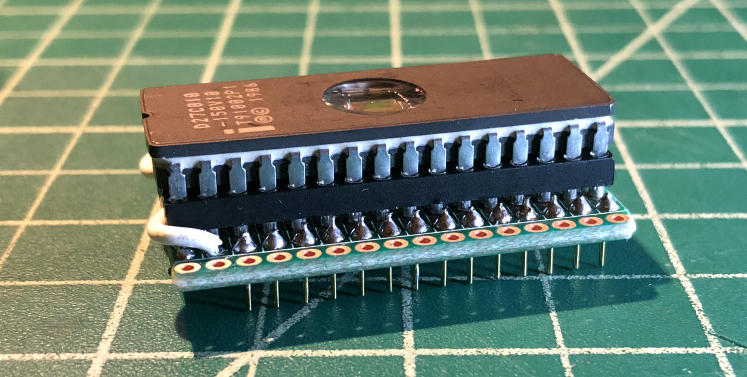
While this works (it boots MS-DOS, and much faster than two separate EPROMs, I might add), it's much too tall for the shallow ROM bed. So, the next step is figuring out something that does fit.
And, here is a listing of the hex file used in testing. It has some miscellaneous DOS files and some GRiD supplied diagnostics.
| FILE | SIZE |
|---|---|
| SYSTEM FILES | 68377 |
| ANSI.SYS | 1989 |
| ASSIGN.COM | 1523 |
| CHKDSK.EXE | 9680 |
| GRIDSCAN.EXE | 12082 |
| SHOWMEM.EXE | 3618 |
| T.COM | 4096 |
| DEVICES.EXE | 2640 |
| DISKCOPY.EXE | 4139 |
| FORMAT.EXE | 11160 |
| MODE.EXE | 5666 |
| TOTAL | 124826 |
That is unless, the protrusion of the ROMs from their special cavity does not bother you. In which case, one could forgo the socket and brand cover altogether. (But, I believe it voids the TEMPEST rating). ↩︎
At least, that I've found. Or rather, are generally found on popular auction websites. ↩︎
Right, well I guess it could have just been cheaper to use EPROMs, so that's not a terribly strong argument. ↩︎
Horowitz, P. and Hill, W. (1989). The art of electronics 2nd ed. Cambridge: Cambridge University Press, p. 502. ↩︎
Triebel, W. and Singh, A. (1991). The 8088 and 8086 microprocessors. Englewood Cliffs, NJ: Prentice-Hall, p.309 ↩︎
Horowitz and Hill, The art of electronics, p. 675. ↩︎
The data lines are named differently as the 27512, being an EPROM, needs both input and output lines. ↩︎