Don't do it the hard way
Semiconductor memory manufacturers offered pin-compatible chips, why not use them?
Well, because installing an EPROM with soldered pins and jumper wires is gross.
But, the important pins do match and that means no pin needs a one-to-one swap with any other. Any jumper added is only to route VCC or VSS. And, as the pins which do require jumpers are, for the most part, outside the 28-pin footprint of the socket, their toing and froing can be confined to the edges of the EPROM, and therefore kept from contributing any additional height to the seated package. And that's important.
The obvious downsides are labor and aesthetics; this method requires some careful and creative soldering and the finished product is, in my experience/opinion, far from beautiful.
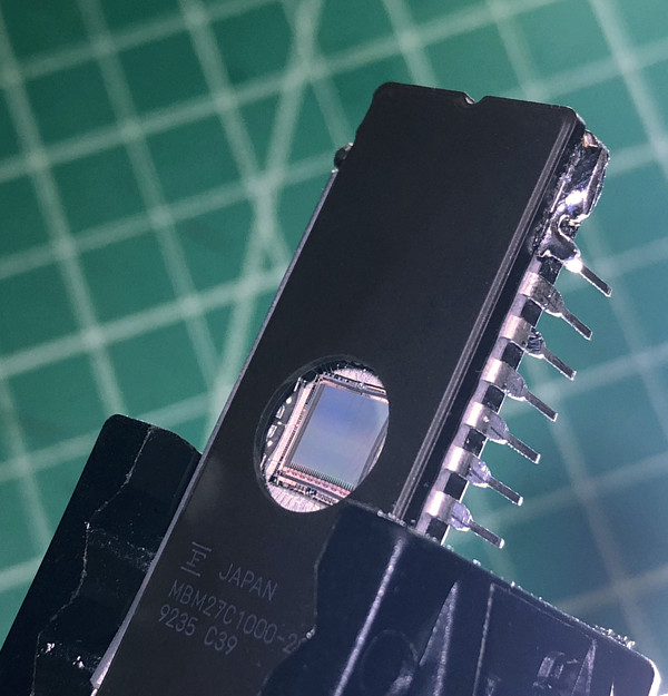
As for the pin-compatibles, I've been able to find references to several part numbers in different databooks, some even available on popular auction websites.
| Manufacturer | Part Number |
|---|---|
| Fujitsu | MBM27C1000 |
| Hitachi | HN27C301 |
| SGS-Thomson | M27C1000 |
| Toshiba | TC571001 |

The connection diagram looks much like that of the pin-incompatible EPROMs; VPP and P̅G̅M̅ are tied to VCC, then the whole bunch is routed to NC on pin 30, which conveniently aligns with VCC on the 28-pin ROM socket.
Since the pin-compatibles' A16 is already in the right place vis-à-vis the socket (swapped with O̅E̅), the only remaining connection to make is from pin 2 to 16. This is VSS on both EPROM and socket.
Side Note:
Unless I miss my guess, pin 30/NC is not internally connected, i.e., one can connect it to ground, or any other pin, or nothing at all. But, I've found that not always to be the case. Sometimes the TGC has refused to recognize an EPROM which uses pin 30 as a conduit for VCC.
Most likely, the root cause is user error. Perhaps I'd relied too heavily on simple solder bridges or the like.
Surgery
The top four pins on the 1M EPROMs need to be pried up and prepped for soldering. Eventually, they'll be clipped, and that raises an important point about this method.
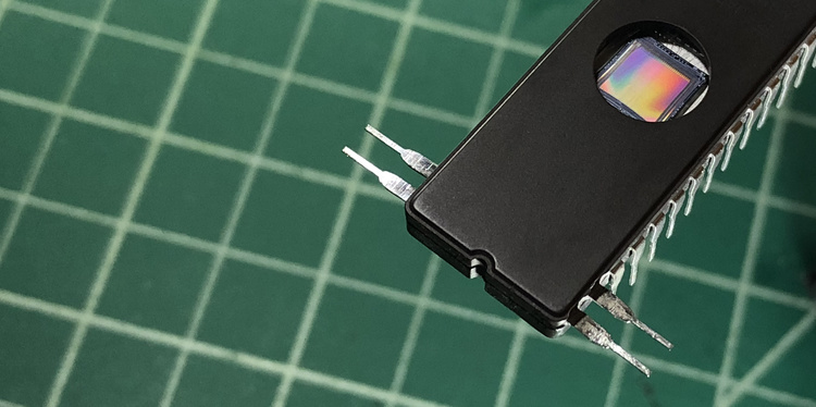
These EPROMs will necessarily become OTP EPROMs. And while that might seem like a good reason/excuse to find (and purchase) some actual OTP EPROMs, as they were predominately made and are invariably found in PDIP packages, performing surgery on them with a hot iron comes with a decreased margin for error.
Depending upon one's steadiness of hand, of course.
Once the pins have been connected and tested for continuity, they're clipped to taste and protected (concealed) with some heat shrink tubing.
The tubing isn't required, but considering the amount of exposed leads on the ROM board, and their proximity to the EPROM's overlapping top end, it seems a reasonable precaution.
Not to mention the hideous solder lumps.
A Note on Programming
For whatever reason, the ubiquitous budget programmer TL866II does not support any of the pin-compatibles.[1] So, unless another adapter is handy, for converting the EPROMs back to a 27C010-style pinout, a different programmer is required. I found that Needham's EMP-20 could handle all the chips listed above.[2]
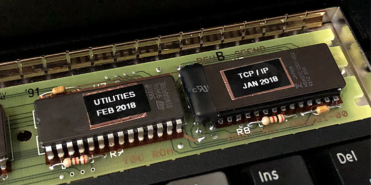
Luckily, the space between each socket is just enough to fit a full complement of 32-pin EPROMs, or a combo of 28- and 32-pin, installed side by side.
However, my opinion is that this is not a long-term solution.