Putting It to Bed
Recap
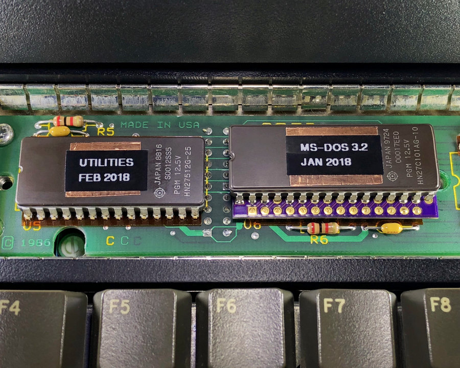
The TGC (TEMPEST GRiDCase)'s expansion board, which enables the end-user to install their own ROMs, has 28-pin sockets and a very low ceiling.[1] The former limits the pin count and capacity of any installed EPROM while the latter restricts the height of any adapter which could facilitate the usage of larger EPROMs.
Also, the higher capacity EPROMs tend to be, in my testing, a bit taller than their 64KB cousins.
While there are solutions available which both require less time and energy and also achieve approximately the same result, I believe that an adapter which does not mutilate the EPROM is preferable.[1:1]
All of which is to say that a "drop-in" replacement would be the ideal.
Eagle CAD
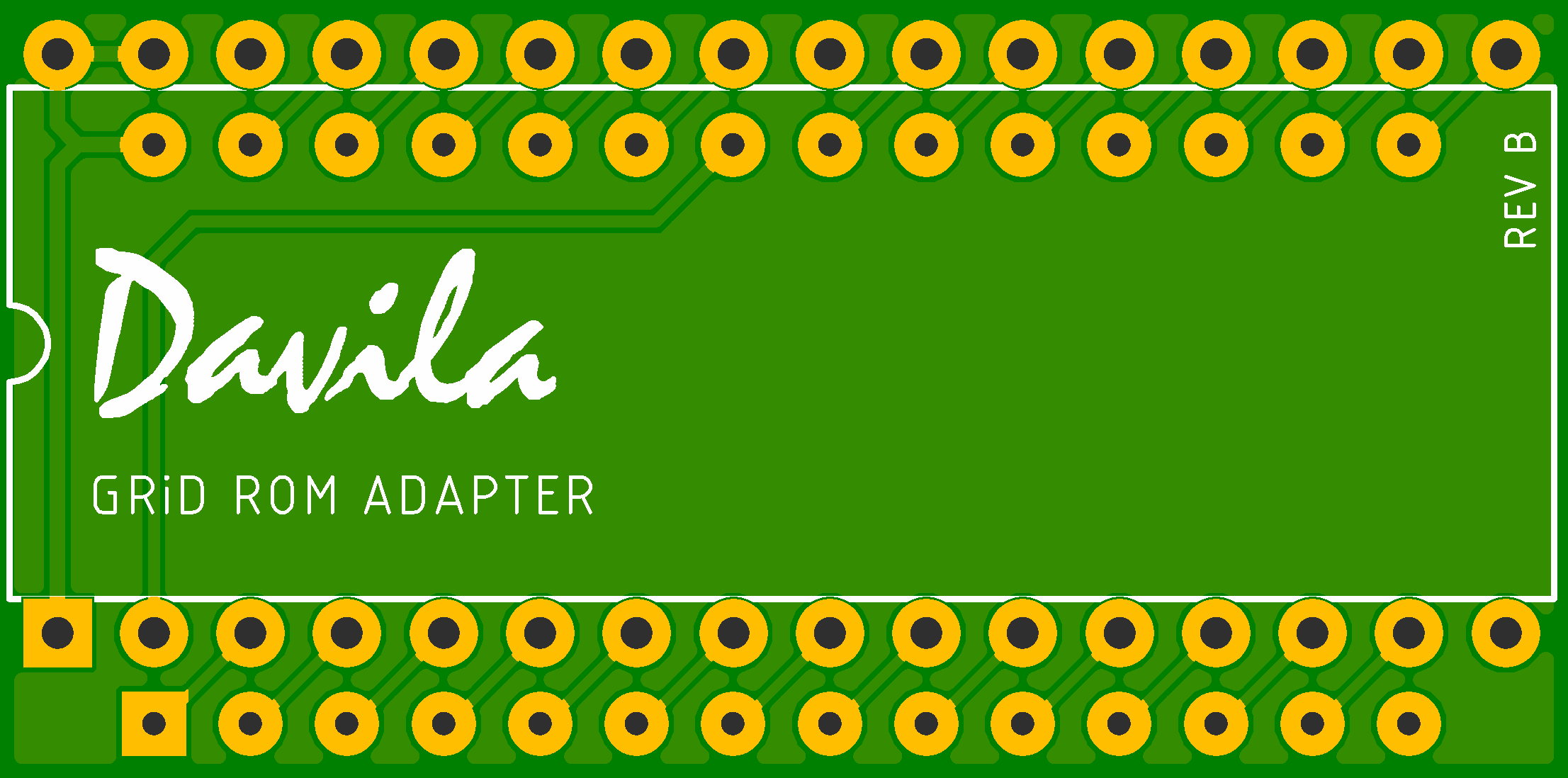
The design of the adapter is not terribly complicated as it's almost a one-to-one match between most of the pins on the two packages. Conveniently, Eagle CAD has both a 27010 and 27512 within its "Generic Memories" library. [1:2] However, using these require modifications to both devices' symbol and package.
The symbols require roughly the same changes. Since Eagle's 27512 will not be representing an EPROM device, but actually a socket, its symbol must be given VSS and VCC. And, even though Eagle's 27010 device does correspond to a real EPROM, VSS, VCC, and NC must be added to its symbol as well. Without these additions, the nets within Eagle's schematic interface cannot be connected and that cascades into issues when laying out the board.
It was clear early on that due to the extremity of the ROM compartment's height constraints, as well as the small diameter of the socket's individual receptacles, any board design which hoped to fit would require speciality pins soldered directly to it, (rather than any of the "low-profile" or "ultra low-profile" sockets offered by different manufacturers).
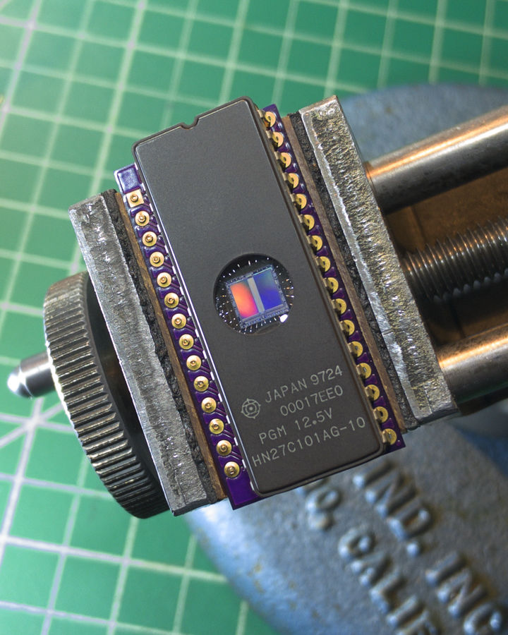
The finished board uses MILL-MAX's 3157 Press-Fit PCB Pins. As their name might suggest, these pins are meant to be pressed into plated through holes on a PCB, slowly, with uniform force, and with lubrication to prevent cold-welding (read: using a piece of industrial machinery which I do not possess).
But, given these pins' basic theory of operation, (that there is a knurled portion on the head of each one which, given enough force, will cut into the metal of the plated hole), I assume most would come to same conclusion as me: That sounds like a job for a hammer.
And indeed it was!
(As well as a pin vise to hold the pins in place).
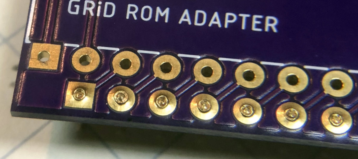
The impact on the plated through holes is visible under magnification, but the connections are good; three boards received the hammer treatment and all three pass continuity tests.
The severity of the holes' deformation may have been the result of --100% was the result of -- my inexplicable decision to set the drill sizes for the pads on the 27512 package to 23.6 mil instead of 0.026 in., even though MILL-MAX very clearly states "mount in a Ø.026 in. hole" And, while it all worked, I would hew closer to the manufacturer's specifications in any further revisions.
The Board
After one and then another design returned from OSH Park, both and increasingly within the horizontal constraints of the daughterboard (as I reduced the overall footprint of the board each time), the prime obstacle remained; Even with the bottom of the adapter flush against the daughterboard, the ROM compartment's cover refused to close.
This precipitated a spree of measuring the heights, both in and out of socket, of every 1M EPROM available to me.
Not only did this lead to a list of EPROM specifications which has no use to anyone other than myself, but also to a newfound appreciation for the min/max values given in datasheets.
One more design was sent to OSH Park, but this time opting for their "2oz Copper with 0.8mm FR4" service, which I'd previously overlooked. The turnaround is understandably longer as each panel needs to collect enough orders to be fabricated (same as their normal two-layer boards) but demand is obviously lower.
I was very pleased with the results, especially as I began attacking them with a dead blow hammer.
The rest of the operation is straight-forward: (1) pick the EPROM with the lowest seated height available, (2) burn files to it, (3) maybe a test before soldering it into the adapter, (4) solder it to the adapter.
Much like the pin-compatibles, any EPROM used in this adapter will mate with it for life, so perhaps a test before installing it is more than a "maybe"
Further Questions:
What are the implications, if any, of manually bending the EPROM's leads so that it can sit absolutely flush against the adapter board?
Or enlarging the drills so that the EPROM can sit flush without bending the leads?
Why not make use of the same memories, but in a smaller package like PLCC32?
Well, if you're already going to be soldering SMD components, what about a 27C010 TSOP? That would definitely be under the height constraints, even with 1.6mm board.
As the ROM daughterboard is removable, why not recreate it, but with its layout adjusted for larger memories?